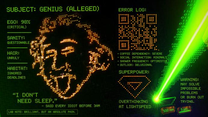
Scientists Sculpt Einstein Onto a Crystal Using Only Light, Because Why Not?
Researchers use light to permanently etch a tiny Einstein portrait into a crystal, showcasing a material that could revolutionize photonics by being its own nanoscale art studio and factory.
Researchers from the XPANCEO Emerging Technologies Research Center, in collaboration with Nobel Laureate Prof. Konstantin Novoselov, have discovered that the crystalline van der Waals semiconductor arsenic trisulfide (As2S3) exhibits a remarkably strong photorefractive effect. This means low-intensity ultraviolet light can permanently alter its refractive index - by up to Δn ≈ 0.3, a change that surpasses those in classic materials like BaTiO3 or LiNbO3 - without needing expensive cleanrooms or fancy femtosecond lasers.
This property allows optical functions to be directly 'written' into the material, a handy trick for creating the tiny structures in telecom systems, compact optical components for sensors, and hologram-like features for security. The effect is so potent at the nanoscale that it can create unique, hard-to-replicate 'optical fingerprints,' ideal for anti-counterfeiting.
To showcase this precision, the team used a standard laser to etch a microscopic portrait of Albert Einstein onto a thin piece of As2S3, with points spaced a mere 700 nanometers apart. They've even pushed the resolution to ~50,000 dots per inch (about 500 nanometers between points), producing patterns with strong optical contrast thanks to the light-induced changes.
Beyond just patterning, exposure to light makes As2S3 physically expand by up to 5%, enabling the direct formation of optical structures like microlenses and diffraction gratings on its surface. This is crucial for developing components like wide field-of-view waveguides for augmented reality glasses and smart contact lenses.
Valentyn Volkov, Founder and CTO at XPANCEO, noted that discovering such sensitive natural crystals provides the 'essential building blocks' for a new generation of light-driven technology, moving photonics forward from its electrical roots. The material's responsiveness also makes it promising for photonic circuits and nanoscale sensors, marking a significant step in manipulating light for next-gen tech.
The Good Times
News in your inbox.
One sardonic roundup, delivered on your schedule. Free. Unsubscribe whenever your tolerance for wit runs out.
Already subscribed but we never reach your inbox? Check your spam folder and hit 'Not spam' (or 'Remove from spam') to bust us out of junk-mail purgatory. You'll be helping everyone else too.
Don't open any of our emails for a month and you'll be automatically removed from the mailing list.
Rewrite Article
Select parts to regenerate with a fresh AI pass. Translations will be updated automatically.
Generate AI Image
Creates a sardonic version of the article image using OpenAI.